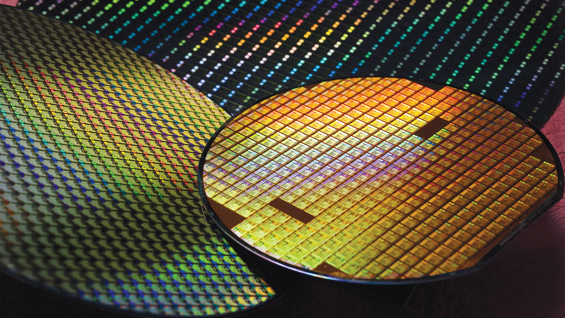
Semiconductors are fundamental components of modern electronics, enabling the operation of devices ranging from microprocessors to solar cells. Understanding how semiconductors work is crucial to grasp the principles that underpin the functioning of electronic devices. This article provides a simplified explanation of how semiconductors work and the key concepts that govern their behavior.
1. Atomic Structure and Energy Bands
At the heart of a semiconductor’s behavior lies its atomic structure. Semiconductor materials, like silicon, have a crystalline lattice composed of atoms with four valence electrons. These valence electrons form covalent bonds, sharing electrons with neighboring atoms.
In a pure semiconductor at absolute zero temperature, all valence electrons are tightly bound in the valence band, and the conduction band remains empty. The valence band represents the highest energy level at which electrons reside, and the conduction band represents the lowest energy level where electrons can move freely.
2. Bandgap and Conductivity
The energy gap between the valence band and the conduction band is known as the bandgap. In insulators, this gap is substantial, making it difficult for electrons to jump to the conduction band. In conductors, there is virtually no bandgap, allowing electrons to flow easily between the bands, resulting in high conductivity.
Semiconductors, however, have a small bandgap, which allows them to exhibit both conductive and insulating properties. At room temperature, some electrons acquire enough thermal energy to bridge the bandgap and move to the conduction band, leaving behind positively charged holes in the valence band. This phenomenon is known as electron-hole pair generation.
3. Doping: Modifying Semiconductor Properties
Doping is a process where impurities are intentionally introduced into the semiconductor crystal lattice to modify its electrical properties. There are two types of doping:
- N-type Doping: When a material is doped with atoms that provide extra valence electrons, such as phosphorus, it becomes an N-type semiconductor. The extra electrons in the crystal lattice increase its electron concentration, making it a good conductor.
- P-type Doping: When a material is doped with atoms that create “holes” or electron vacancies, such as boron, it becomes a P-type semiconductor. The presence of holes allows for easy movement of positive charge carriers, creating conductivity.
4. PN Junctions and Diodes
A PN junction is formed when a P-type semiconductor comes into contact with an N-type semiconductor. At the junction, electrons from the N-side diffuse to the P-side, and holes from the P-side diffuse to the N-side. This migration results in the formation of a depletion region, an area depleted of charge carriers.
When a forward bias voltage is applied across the PN junction, it narrows the depletion region, allowing electrons and holes to combine and create a conducting path. This results in a low resistance path for current flow, making the PN junction conductive. This is the principle behind a diode, a semiconductor device that permits current flow in one direction only.
Conclusion
Semiconductors are vital components that drive the world of modern electronics. Their ability to switch between conductive and insulating states, modifiable through doping, makes them invaluable for various applications. By understanding the fundamental concepts of electron behavior, energy bands, and PN junctions, we gain insight into how semiconductors function, enabling the design and development of ever more advanced electronic devices that power our technological age.
